In the structural AI boom of 2026, memory chips have evolved from a commodity that follows the market to a core strategic asset that determines survival in the AI era. The epicenter of this transformation is the battle over high-bandwidth memory () manufacturing processes.
The Physical Breakthrough of the Computing Bottleneck: From Memory Wall to Agentic Workloads
1.1 The Physical Limits of the Memory Wall and Architectural Evolution
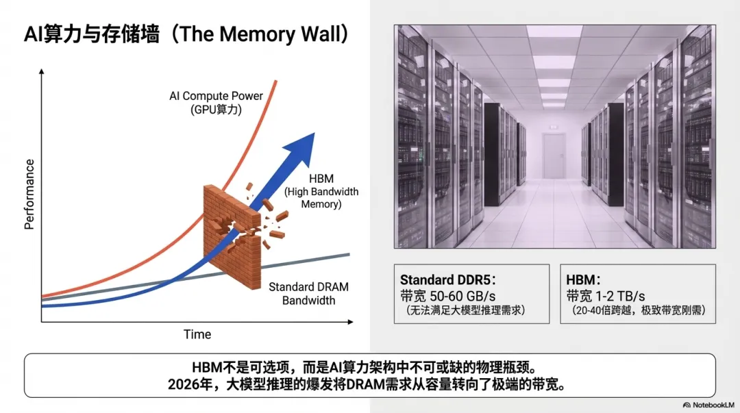
The most severe challenge facing current computing systems is the extreme imbalance between processor compute power and memory bandwidth, known as the memory wall. Over the past two decades, logic processor performance has improved about 60,000 times, while standard DRAM bandwidth has only increased about 100 times. This bandwidth gap is magnified infinitely in the generative AI era, as large language models need to frequently read hundreds of billions of parameter weights from memory during inference. When the memory system cannot supply data at a rate matching the processor, powerful compute cores stall, causing a sharp drop in system energy efficiency.
To break this bottleneck, HBM technology uses through-silicon vias () to vertically stack DRAM chips. This 3D integration architecture creates thousands of microscopic vertical data highways inside the chip, delivering ultra-wide bus bandwidth of 1 to 2 TB/s—a 20x to 40x leap over traditional DDR5 memory. By 2026, high bandwidth has shifted from a nice-to-have to a hard physical requirement for large model inference.
1.2 From Chatbots to Agentic AI: The Workload Transformation
The fundamental shift in AI workloads in 2026 is the deeper driver of memory technology change. In 2023-2024, AI demand was mainly human-paced: user input, bot output. But with the explosion of agentic AI, systems now run continuous, autonomous loops. These agents, upon receiving a single instruction, automatically plan, execute, check, and correct, causing internal reasoning steps and data throughput to grow exponentially. Monthly token generation has surged from about 40 trillion in 2024 to about 4 quadrillion by end-2025—a nearly 100x increase. This high-intensity computing puts extreme pressure on the already fragile memory link. AI is no longer just a software tool; it has become a 24/7 computing infrastructure, requiring memory chips with not only extremely high bandwidth but also excellent stability and thermal dissipation.
Chapter 2: The Physical Battle at the Process Peak: TC-NCF vs. MR-MUF
The core of HBM manufacturing is fighting extreme heat and physical stress at the nanometer scale. In the 2026 market, yield control has become the dividing line for survival. Currently, the memory industry has split into two paths: Samsung's TC-NCF and SK Hynix's MR-MUF. Their technical differences determine profitability in the 12-layer (12-Hi) and 16-layer (16-Hi) stacking era.
2.1 Samsung: TC-NCF's Persistence and Physical Challenges
Samsung, the traditional memory king, has deep expertise in thermal compression non-conductive film (TC-NCF). The process places a solid non-conductive film (NCF) between DRAM chips, then applies extreme heat and pressure from a top thermal head to melt and cure the film, fixing the chips in place.
However, as stacking layers increase to 12 or even 16, this process hits severe physical limits. First, the heat trap effect: gaps in the solid film layers make it hard for internal heat to conduct vertically, causing temperature buildup. Second, the layer-by-layer thermal compression process, when handling ultra-thin silicon wafers, easily causes physical warpage due to uneven heating. In 16-layer stacking, millimeter-scale film thickness errors often cause TSV breakage. These factors made Samsung's HBM3E yield ramp extremely difficult; by Q2 2025, its HBM market share had fallen to 17%.
2.2 SK Hynix: MR-MUF's Efficiency Lead
SK Hynix, with its mass reflow molded underfill (MR-MUF) process, has established a clear competitive advantage in the HBM3 and HBM3E eras. The core of this process is to pre-stack all DRAM chips precisely, then inject liquid epoxy (MUF) to fill the gaps in one shot, followed by a single batch curing step.
MR-MUF is the thermal management king at this stage. The liquid material fills gaps seamlessly, improving thermal conductivity by over 20% compared to NCF. Because it uses batch reflow, pressure distribution is extremely uniform, completely solving the silicon warpage problem in high-layer stacking and achieving very high yields. This process barrier allowed SK Hynix to surpass Samsung in operating profit for the first time in 2025 and capture 62% of the global HBM market.
2.3 Comparison of Technical Routes and Economic Consequences
| Technical Indicator | Samsung TC-NCF | SK Hynix MR-MUF |
|---|---|---|
| Material Form | Solid non-conductive film | Liquid epoxy resin |
| Packaging Flow | Layer-by-layer thermal compression (slow) | Batch reflow & molding (efficient) |
| Thermal Performance | Structural thermal resistance bottleneck | >20% better heat dissipation |
| 16-Layer Yield | High warpage & TSV breakage risk | Strong physical stability, higher yield |
| Q2 2025 Market Share | ~17% | ~62% |
Chapter 3: The Capacity Vampire Effect: AI's Bloodletting of Consumer Electronics
In the silicon economics of 2026, HBM expansion comes at a cost. The memory industry is undergoing a structural reallocation known as the 1:3 capacity vampire effect.
3.1 HBM's Production Resource Consumption Logic
Manufacturing one HBM wafer consumes about three times the core production resources of a standard DDR5 wafer. This disproportionate resource usage stems from HBM's very low bit density output: larger die area penalty, extreme complexity of TSV processing, and yield loss from increased stacking layers.
By 2026, HBM is expected to consume about 25% of global DRAM wafer starts. This means that even if total wafer starts remain constant, the actual bit output of standard memory for PCs, smartphones, and general servers will shrink sharply. This is vividly called the vampire effect: AI is sucking the lifeblood out of other electronics markets.
3.2 Price Shock and Shipment Contraction in End Markets
This capacity reallocation directly causes structural shortages in the standard memory market. In Q1 2026, DRAM contract prices surged 50-55%, with some specific categories up 180%. This cost pressure is mercilessly passing downstream:
In PCs, memory's share of total BOM cost jumped from 16% in 2025 to 23%, and up to 35% for some high-performance models. This forces manufacturers into a dilemma: protect market share or protect margins. Gartner expects global PC shipments to shrink 10.4-11.3% in 2026. In smartphones, models below $500 face severe survival challenges due to rising memory costs. Some entry-level models have been forced to cut specs or raise prices sharply; 2026 smartphone shipments are expected to shrink 8.4-12.9%.
3.3 Paradigm Shift in Memory Valuation
Traditional memory chips were seen as strongly cyclical commodities, valued on P/B mean reversion. But in 2026, with HBM becoming a core component of long-term infrastructure, valuation logic is shifting toward growth premiums.
Micron forecasts the HBM market will explode from $35 billion in 2025 to $100 billion by 2028—equivalent to the entire global DRAM market in 2024. Investors no longer focus only on inventory turnover; they now watch market share in high-value products and technology leadership. The market is accepting 20-30x forward P/E, rather than the 5-8x at traditional cycle peaks.
Chapter 4: The Capital War: Hyperscaler Capacity Buyouts and Debt Expansion
By 2026, AI infrastructure buildout has become a capital war that consumes cash at an unprecedented rate. Global hyperscalers are locking up memory chip capacity on a historic scale.
4.1 Capacity Buyouts and Long-Term Contracts
Microsoft, Meta, Google, and Amazon (AWS) have bought out HBM capacity for the next two years with massive prepayments. These orders are highly exclusive, and spot market pricing power has been completely bypassed. SK Hynix and Micron have publicly confirmed that their 2026 HBM capacity is fully sold out, with order visibility extending into 2027. This demand is not short-term consumer fluctuation but rigid infrastructure investment. In this environment, memory makers with advanced capacity hold absolute bargaining power; pricing authority has reversed from downstream OEMs back to the top three chip giants.
4.2 Massive Spending and Debt Risk
In 2026, the top five hyperscalers' combined capex is expected to reach $660-690 billion, nearly double 2025 levels. This spending intensity has reached 45-57% of their total revenue—unprecedented in tech history. To bridge the gap between operating cash flow and aggressive spending, these historically asset-light tech giants are tapping debt markets heavily. In 2025 alone, they raised over $100 billion in bonds, with total debt expected to reach $1.5 trillion in the coming years.
| Company | 2026E Capex | vs 2025 | Core Focus |
|---|---|---|---|
| Amazon | ~$200B | ~51% | AWS data centers, custom AI chips |
| Alphabet | $175-185B | ~100% | TPU expansion, optical network infrastructure |
| Microsoft | >$120B | ~36% | Azure compute clusters, OpenAI partnership |
| Meta | $115-135B | ~75% | Llama model training, superintelligence lab |
| Oracle | ~$50B | ~138% | OCI cloud expansion |
4.3 The Capex Cliff Risk
Despite the steep spending curve, potential secondary risks are alarming financial markets. If AI monetization (software subscriptions, business efficiency) fails to materialize as expected, massive fixed-asset depreciation will hit income statements hard. If orders are cut, this high-leverage capital expansion could quickly turn into a debt-driven crash. Credit default swap (CDS) markets have already priced in higher protection costs for tech giant bonds, reflecting investor concern over this risk premium.
Chapter 5: Upstream Bottlenecks: Specialty Materials and Equipment Supply Constraints
The HBM manufacturing game is not just about the three memory makers; the entire supply chain's resilience is under severe test. Some monopolistic specialty material suppliers have become the key bottleneck limiting capacity expansion.
5.1 Nitto Boseki's Glass Cloth Monopoly
High-layer HBM chips require highly stable substrates, with the key material being specialty glass fiber cloth. This niche is absolutely dominated by Japan's Nitto Boseki, which holds a 90% global market share in high-end low-CTE glass cloth. With AI servers' surging demand for high-performance PCBs and substrates, Nitto Boseki's capacity is maxed out. This glass cloth not only affects chip heat dissipation but is also critical to preventing substrate warpage during high-layer stacking. The production process involves precise chemical treatment and special weaving, making capacity expansion very slow. Apple and Nvidia procurement teams have made multiple trips to Japan to coordinate supply, but industry estimates suggest Nitto Boseki's capacity gap will persist until end-2027. Without substitutes, even if Samsung or Hynix have plenty of wafers, they cannot turn them into final products without this material.
5.2 Etching and Test Equipment Delivery Pressure
Beyond materials, the delivery speed of TSV etching equipment and ultra-thin wafer grinding tools directly constrains memory makers' ramp-up. Japanese equipment makers like Disco have order backlogs for laser cutting and grinding tools stretching years out. These tools must operate in vacuum and extreme precision to thin DRAM wafers to about 30 microns without breakage. Additionally, ASML's lithography supply remains tight. Since 1c DRAM (6th generation, 10nm-class) requires more EUV exposure steps, delivery delays will directly postpone Samsung's 1c node mass production.
Chapter 6: The Endgame: Blurring Foundry Boundaries and Heterogeneous Integration
Looking ahead to HBM4 and beyond, the memory industry's organizational structure is undergoing fundamental change, with the traditional IDM model shifting toward ecosystem collaboration.
6.1 External Foundry Trend for Logic Base Die
In the HBM4 era, to achieve extreme bandwidth of 2TB/s, 16-layer stacking is already pushing physical limits. The biggest change is the blurring of foundry boundaries: the base die for HBM4 will no longer be made by memory makers alone but will shift to foundries like TSMC using 12nm or even 5nm advanced processes. The deep logic: as memory wall pressure moves inside the chip, the base die needs more complex logic control circuits for data preprocessing. SK Hynix's deep alliance with TSMC aims to leverage TSMC's dominance in advanced logic foundry to gain performance and power advantages in memory stacking. This means memory chips are transforming from standardized commodities to highly customized heterogeneous integrated components.
6.2 Samsung's Full-Stack Integration Counterattack
Facing SK Hynix's ecosystem alliance, Samsung is trying to use its full-stack integration advantage for a curveball. Samsung is the only company that can simultaneously provide 1c DRAM memory layers, 4nm logic base dies, and advanced 3D packaging services. In early 2026, Samsung demonstrated its 12-layer and 16-layer HBM4 physical chips, with single-pin speeds of 11.7-13 Gbps and single-stack bandwidth up to 3.3 TB/s—2.7x the previous generation. Through internal logic foundry and memory division co-optimization (DTCO), Samsung aims to build a moat in power management. Additionally, Samsung is aggressively adopting hybrid bonding in 16-layer stacking, using copper-to-copper direct interconnection to eliminate traditional micro-bumps, improving thermal efficiency by 30%. Although hybrid bonding yields are still around 10%, this is seen as the key technology reserve that will determine the competitive crown after 2028.
6.3 HBM4 Roadmap Evolution Analysis
| Metric | HBM3E (Current) | HBM4 (2026 Production) | HBM4E (2027-2028E) |
|---|---|---|---|
| Single-Stack Bandwidth | 1.15-1.2 TB/s | 2.0-3.3 TB/s | Up to 4.0 TB/s |
| Memory Interface Width | 1024-bit | 2048-bit (doubled) | 2048-bit |
| Packaging Process | MR-MUF or TC-NCF | MR-MUF / hybrid bonding trials | Hybrid bonding (HCB) mainstream |
| Logic Base Die Node | Memory-specific node | 12nm / 5nm logic node | 5nm / 3nm / 2nm |
| Max Stacking Layers | 12-Hi | 16-Hi | 16-Hi / 20-Hi |
Chapter 7: Geopolitical Chess: Memory as a Strategic Asset
In the complex macro environment of 2026, memory chips have transcended commerce and taken on national security attributes.
7.1 US Onshoring and Micron's Role
Micron, as the only US-based memory IDM, is receiving unprecedented policy support. With the CHIPS Act, Micron's mega-fabs in New York and Idaho are accelerating. In 2026, Micron has taken an extreme contraction strategy: completely shutting down its Crucial consumer line and shifting 100% of capacity to enterprise and AI. This strategic pivot should lift its HBM market share back above 25% by end-2026. As a core asset for US computing security, Micron has a natural advantage in winning government contracts and meeting US data center compliance.
7.2 Technology Blockade and Chinese Players' Struggle
US restrictions on China's access to advanced memory technology tightened further in 2026. Since HBM manufacturing requires advanced packaging equipment and 10nm-class DRAM production lines, both under export controls, Chinese players like CXMT and YMTC face huge difficulties in catching up on high-performance HBM. However, this blockade is forcing Chinese firms to seek scale breakthroughs in mature processes. Their concentrated capacity release in DDR4 and low-layer NAND could cause price shocks in global traditional memory markets, further squeezing traditional IDM margins. Meanwhile, China is accelerating R&D of domestic substrates and packaging materials, trying to achieve supply chain resilience in bottleneck segments like glass cloth.
7.3 The Korea-US Capacity Migration Dilemma
Korean memory giants face an awkward geopolitical dilemma. The US Commerce Department has repeatedly hinted that Samsung and Hynix must build memory fabs in the US to avoid high tariffs. But for Korea, advanced memory technology is a core national strategic pillar, and the Korean government is extremely cautious about approving technology outflows. Moreover, the US lacks skilled semiconductor technicians, and operating costs there are more than double those in Korea. Forced fab construction in the US could severely damage memory makers' gross margins. This conflict of interest has led to a split capacity expansion rhythm in 2026: core R&D and the most advanced production lines stay in Korea, while relatively mature or packaging-only stages migrate to overseas sites like Indiana.
Chapter 8: End-Market Alternatives: AI PCs and On-Device Intelligence
As data center compute costs and bandwidth pressure continue to rise, from H2 2026, the trend of shifting compute to the edge is becoming more apparent. This creates new demand for low-power, high-bandwidth memory.
8.1 LPDDR6 Mass Production and On-Device Inference
To run local AI agents smoothly on phones and laptops, low-power memory standards are leaping. SK Hynix has demonstrated LPDDR6 based on the 1c node, with peak transfer rates of 14.4 Gbps—33% faster than LPDDR5X. Samsung focuses on ultra-low voltage, achieving 12.8 Gbps at 0.97V while cutting read power by 27%. This low power is key to AI PCs maintaining long battery life. By end-2026, with the普及 of on-device compute, the strongest global consumer electronics replacement cycle since 2010 is expected. Despite higher unit costs, consumers may still buy due to the functional leap.
8.2 The Commercialization Year of Processing-in-Memory (PIM)
To fundamentally solve the memory wall, SK Hynix is pushing processing-in-memory (PIM) technology. Its LPDDR6-PIM is optimized for large language model inference, performing basic matrix multiplication inside the memory itself, cutting total system power by 20%. This technology transforms memory from a passive data mover into an active computing participant, marking a certain end to the von Neumann architecture in silicon economics.
Chapter 9: Risk Assessment and Conclusion
In the 2026 macro view, nanometer-scale thermal management differences have reshaped oligopoly structures in a hundred-billion-dollar market. But the cracks beneath the prosperity deserve deep analysis.
9.1 Persistence of Structural Imbalance
The current high memory prices and end-market contraction are not short-term cyclical fluctuations but a long-term new normal from the underlying computing architecture upgrade. As long as AI inference intensity remains on its current slope, the capacity squeeze on standard DRAM cannot be resolved before 2027 through new cleanroom construction. This means global consumers will have to pay for the cloud computing feast for the next two years.
9.2 Risk of Technology Path Dependency
SK Hynix's heavy reliance on MR-MUF has made it profitable in the short term, but if Samsung can overcome hybrid bonding yield issues by 2028, the current technology advantage could quickly become a liability. Hybrid bonding's potential in signal integrity and thickness control makes it the only ticket for stacking above 20 layers.
9.3 Political Consequences of Silicon Economics
The reallocation of semiconductor capacity has caused extreme concern among governments about their electronics industry lifelines. When memory chips go from a commodity to a strategic resource that must be fought for, the global supply chain's efficiency-first principle has completely given way to security-first.
In conclusion, in the silicon world of 2026, whoever masters advanced packaging processes (physical heat dissipation and yield) and advanced manufacturing capacity holds the throat of the global AI industry. Memory chips are shedding their label as digital crude oil and becoming the most精密, most expensive, and most strategically valuable silicon cortex in human civilization. In this process, every technology choice a company makes is not just an engineering challenge but a high-stakes gamble determining national fate and business success.
Risk Disclaimer: This article is for informational purposes only and does not represent any investment advice. Markets are risky; invest with caution.

专注投资分析、市场洞察与资产配置。不追短期波动,只理解真正驱动长期回报的东西。